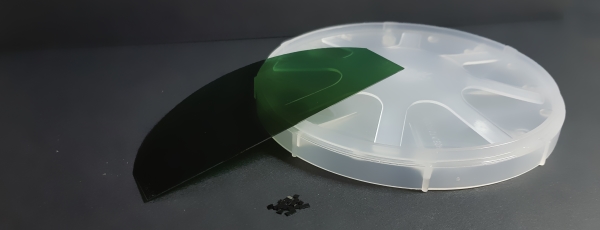
Thermal laser cleaving

Scribing of brittle semiconductor materials

Confirmed for: silicon carbide, gallium nitride

Possible applications: gallium arsenide, germanium, other semiconductor materials

Patents: TW1592242(B), KR101944657(B1), EP3302866(B1) - further applied to GB, IE, DE, FR, NL, BE, LT, RU2677574(C1)

Pending patents: CN108472765(A), JP2018523291(A), US20190139799(A1)

Silicon carbide wafer scribing

 
Evana Technologies owns a patented method for scribing silicon carbide wafers - a very promising material in high power electronics manufacturing industry.
 

READ MORE

Coated silicon carbide wafer scribing

 
A variation of our silicon carbide scribing method for metal coated wafers.
 

READ MORE

COPYRIGHT © 2024 · EVANA TECHNOLOGIES UAB · ALL RIGHTS RESERVED