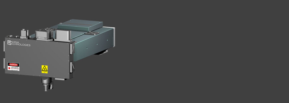
Optical engines for laser scribing
ICICLE sapphire scribing technology
Silicon carbide laser scribing technology
Lithium niobate laser scribing technology
Check out this video about our silicon carbide scribing technology!


 Check out this video about our silicon carbide scribing technology!